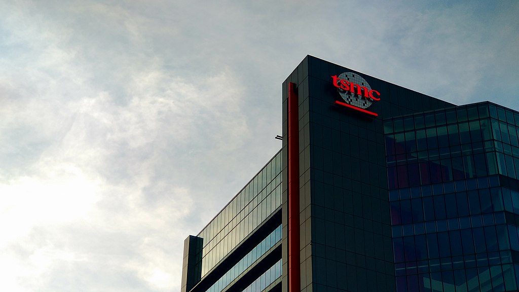
According to undisclosed reports, Taiwan's TSMC is exploring plans to extend advanced packaging capacity to Japan, potentially elevating the country's semiconductor industry rejuvenation.
TSMC Considers Expanding Advanced Packaging to Japan, Potentially Boosting Semiconductor Industry
Taiwan's TSMC is reportedly considering building advanced packaging capacity in Japan, boosting Japan's efforts to revitalize its semiconductor industry, Reuters stated.
They added that the discussions are still in their early stages and declined to be identified because the information was not public. According to one source briefed on the matter, the chipmaking giant is considering bringing its chip-on-wafer-on-substrate (CoWoS) packaging technology to Japan.
CoWoS is a high-precision technology that stacks chips on each other to increase processing power while saving space and lowering power consumption. TSMC currently has all of its CoWoS capacity in Taiwan.
The source stated that no decisions have been made regarding the size or timeline of a potential investment. TSMC, formerly known as Taiwan Semiconductor Manufacturing Co., declined to comment.
Demand for advanced semiconductor packaging has risen globally in tandem with the artificial intelligence boom, prompting chipmakers such as TSMC, Samsung Electronics, and Intel to expand capacity.
TSMC's Ambitious Expansion Plans Signal Japan's Rising Importance in Semiconductor Industry
In January, TSMC Chief Executive C.C. Wei stated that the company intends to double CoWos output this year and schedule further increases for 2025.
Building capacity for advanced packaging would allow TSMC to expand its operations in Japan, where it recently built one plant and announced another on the southern island of Kyushu, a chipmaking hub.
TSMC is partnering with companies such as Sony and Toyota, with a total investment in the Japan venture expected to exceed $20 billion.
In 2021, the chipmaker will open an advanced packaging research and development center in Ibaraki prefecture, northeast of Tokyo.
Japan is viewed as well-positioned to play a larger role in advanced packaging due to its leading semiconductor materials and equipment manufacturers, increasing investment in chip fabrication capacity, and strong customer base.
Photo: Briáxis F. Mendes (孟必思), CC BY-SA 4.0, via Wikimedia Commons


 OpenAI's Desktop Superapp: Unifying ChatGPT, Codex, and Browser Tools for Enterprise AI
  Microsoft Eyes Legal Action as Amazon-OpenAI Deal Threatens Azure Exclusivity
  Google's TurboQuant Algorithm Sends Memory Chip Stocks Tumbling
  Air Canada Express Crash at LaGuardia: Controller Distracted by Prior Emergency
  Elon Musk Announces Terafab: SpaceX and Tesla to Build Dual AI Chip Factories in Austin, Texas
  Palantir's Maven AI Earns Pentagon "Program of Record" Status, Reshaping Military AI Strategy
  Rio Tinto's Resolution Copper Mine: U.S. Smelting Challenges and Global Operations Update
  Sonova Shares Slip as Hearing Aid Giant Lowers Growth Outlook and Plans Sennheiser Exit
  9 Tips for Avoiding Tax Season Cyber Scams
  AWS Bahrain Region Disrupted by Drone Activity Amid Middle East Conflict
  Delivery Hero Sells Taiwan Foodpanda to Grab for $600 Million in Debt-Reduction Push
  Reflection AI Eyes $25 Billion Valuation in Massive $2.5 Billion Funding Round
  Nanya Technology Shares Surge 10% After $2.5 Billion Private Placement from Sandisk and Cisco
  Citi Names Eric Farina and Rob Cascarino to Lead Global Infrastructure Financing Group
  Goldman Sachs Raises ECB Rate Hike Forecast Amid Persistent Energy-Driven Inflation


