


 Trump Criticizes ABC, NBC and CNN for Limiting Coverage of Election Speech
  Stripe, Advent Offer Over $53 Billion to Acquire PayPal in Major Fintech Deal
  Netflix Stock Drops After Weak Q3 Outlook Overshadows Mixed Q2 Earnings
  Eli Lilly Eyes AtaiBeckley Acquisition to Expand Psychedelic Mental Health Pipeline
  UBS Boosts China Tech Bets, Adds Kuaishou and Meituan to Focus List
  Volvo Cars Q2 Profit Falls as Automaker Bets on EX60 EV to Drive Recovery
  NTSB Leads Investigation Into Ryanair Boeing 737 Engine Failure Over Greece
  Seven & i Eyes Żabka Stake in Major European Expansion Push
  NY Times Challenges Trump Administration Subpoenas Over Air Force One Report
  Volkswagen Launches €28,000 ID. Cross EV as Europe’s Electric Vehicle Demand Accelerates
  PayPal Rejects $53 Billion Stripe-Advent Takeover Offer as Too Low: Report
  SpaceX Eyes Pentagon AI Deal as Cloud Pricing Strategy Pressures CoreWeave
  United Airlines Beats Q2 Earnings, Raises 2026 Profit Outlook Despite Higher Fuel Costs
  Jamie Dimon Warns Anthropic's Mythos AI Poses National Security Risks
  Apple Intelligence Cleared for China as Alibaba and Baidu AI Power iPhone Features
  Uber to Acquire Delivery Hero in $14.8 Billion Deal to Expand Global Food Delivery Business


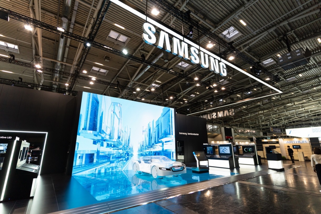
Samsung Electronics is setting up a new semiconductor research facility in Japan near Tokyo. The South Korean firm is reportedly spending $280 million or ¥40 billion on this project.
According to NHK Japan, Samsung Electronics will build its research and development (R&D) hub in the Minato Mirai business district located in the city of Yokohama. The site is expected to be a center for inventing chip-packaging technology for high-performance silicon.
Japanese Government's Subsidy Grant
It was reported that Japan has been continuously working on attracting foreign semiconductor companies so they will open their facilities in the country. This is because the nation sees chipmaking as critical to economic security and would like to boost its local supply chain.
As part of its efforts to entice chipmakers, the Japanese Ministry of Industry revealed it will grant subsidies to Samsung Electronics worth up to ¥20 billion. With this amount, the government covers almost 50% of the total cost of the new R&D facility.
Japan will continue to scale up its chip industry as it looks to support the recovery of domestic chip manufacturing. Prime Minister Kishida Fumio confirmed that the government committed to subsidizing Samsung Electronics for its advanced chip lab in the territory. In any case, Reuters reported that the electronics firm's $280 million investment is set to be distributed over five years.
Details About the New Samsung Research Center
Meanwhile, Korea Joongang Daily mentioned that Samsung Electronics' research center in Tokyo has been named the "Advanced Package Lab" or simply APL. The hub will have a floor space measuring 71,000 square feet and be divided to house the company's research facilities and backup offices. The firm aims to open the lab in 2024 and is expected to hire about 100 new researchers.
"Samsung wishes to fortify leadership in semiconductors through continuous technology research," Samsung's head of chip unit, Kyung Kye Hyun, said in a statement this week. "Yokohama is one of the most suitable locations to collaborate with industries, universities and research centers, as it houses many companies and institutions related to chip packaging."
Photo by: Samsung Media Library


