US 10-Year Treasury Yield at 6% Emerges as New Market Risk Threshold
  Select Water Solutions Shares Surge on $700 Million Pilot Water Deal
  Australia Unemployment Hits Five-Year High Despite Strong Jobs Growth
  Tencent Launches TenPayGo Payment App for Foreign Tourists in China
  SoftBank Shares Fall as Oracle Flags Stargate Data Center Delay Risk
  Fed Unveils Stablecoin Rules Under GENIUS Act
  Airbus Finds A321neo Fuselage Quality Issue
  Russian Envoy Dmitriev Heads to US for Ukraine Talks
  Japanese Bank Stocks Surge as Bond Yields Fuel Rate Hike Bets
  Dollar Holds Near Two-Month High as Yen Approaches 160
  Apple Extends Qualcomm Patent Licensing Deal
  Mercedes-Benz Eyes €800 Million Labor Cost Cuts in Germany
  Japan Private-Sector Growth Slows as Domestic Demand Weakens
  Soybean Futures Slip as Traders Await Trump-Xi Trade Signals
  China’s ‘Lipstick King’ Says AI Won’t Replace Livestream Hosts
  SoftBank Raises $11.1 Billion in Bond Sale to Fund OpenAI Investment
  Former OpenAI Data Center Chief Chris Malone Joins Nvidia


 Add as a preferred source on Google
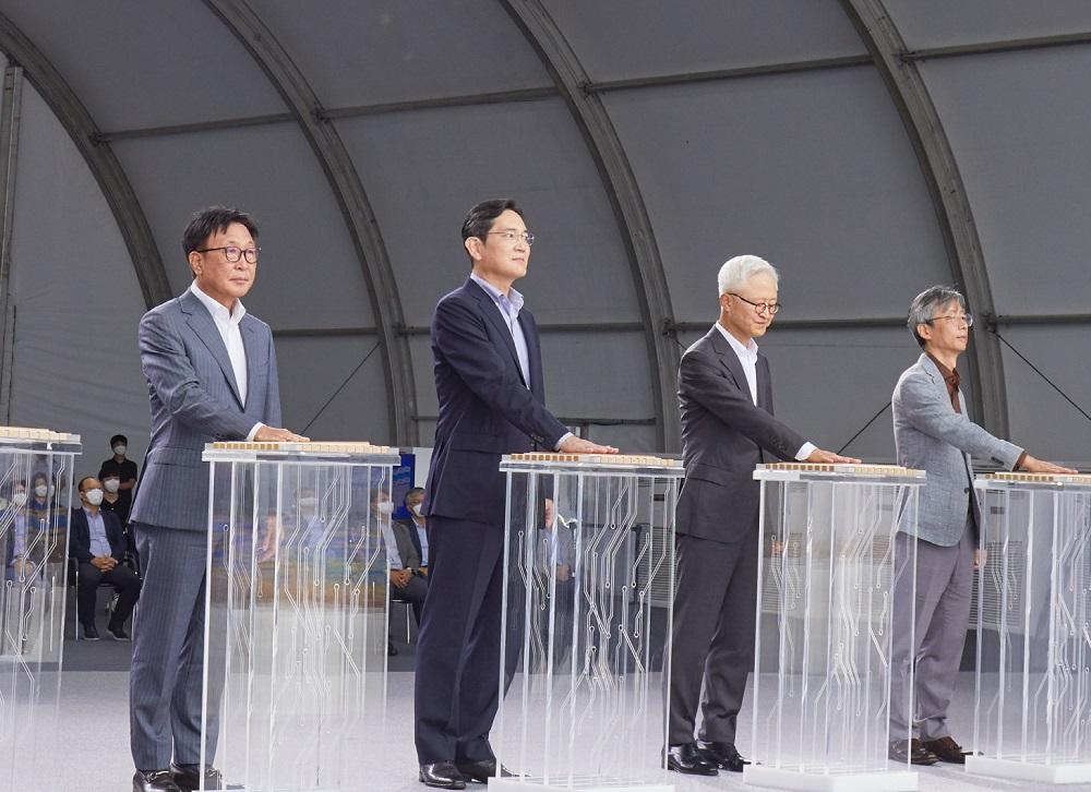
Samsung Electronics Co. is investing KRW20 trillion, or around $15.1 billion, to build its research and development facility for semiconductor products. The company is said to have a goal of catching up with Taiwanese chipmaker, Taiwan Semiconductor Manufacturing Co. (TSMC), as well as tackling competition with other rivals through advanced technology development.
Samsung Electronics is one of the top chipmakers in the world, and it is building a multi-billion R&D complex to bring in a competitive edge in the growing tussle against its rivals. As per The Korea Economic Daily, the tech giant broke ground in Giheung, Yongin, for the construction of its newest facility. It is set to operate a dedicated production line for the R&D hub starting in 2025.
It was noted that Samsung started its chipmaking business in Giheung in 1983 and made major breakthroughs in the business. It also has many achievements, including the development of the world’s first 64Mb DRAM in 1992.
Samsung’s market share gap with TSMC has remained wide in the industry, and its smaller rivals are catching up fast with the leaders in the memory chip business. The smaller companies have been expanding their presence, and they are slowly being recongnized. To act on these issues, Samsung’s vice chairman Lee Jae Yong decided to develop new technologies, and this is what the R&D complex is mainly for.
“Our new state-of-the-art R&D complex will become a hub for innovation where the best research talent from around the world can come and grow together,” Samsung’s president and chief executive officer of the Device Solutions unit, Kye Hyun Kyung, said in a press release. “We expect this new beginning will lay the foundation for sustainable growth of our semiconductor business.”
With Samsung’s new advanced R&D hub in the complex, it is expecting to shorten the development period of chip products on top of improving the quality of its products. The business sectors are hoping that the facility will successfully produce cutting-edge technologies that will not just help Samsung but the entire semiconductor ecosystem of the country.
Meanwhile, The Korea Times reported that Lee Jae Yong was present during the groundbreaking ceremony for the R&D complex. This could be considered his first official activity after being pardoned by President Yoon Suk Yeol last week. This was the executive and Samsung heir’s first public appearance while performing his job.