Missouri Judge Dismisses Lawsuit Challenging Starbucks’ Diversity and Inclusion Policies
  Weight-Loss Drug Ads Take Over the Super Bowl as Pharma Embraces Direct-to-Consumer Marketing
  Baidu Approves $5 Billion Share Buyback and Plans First-Ever Dividend in 2026
  Rio Tinto Shares Hit Record High After Ending Glencore Merger Talks
  Prudential Financial Reports Higher Q4 Profit on Strong Underwriting and Investment Gains
  OpenAI Expands Enterprise AI Strategy With Major Hiring Push Ahead of New Business Offering
  Nasdaq Proposes Fast-Track Rule to Accelerate Index Inclusion for Major New Listings
  SpaceX Prioritizes Moon Mission Before Mars as Starship Development Accelerates
  TrumpRx Website Launches to Offer Discounted Prescription Drugs for Cash-Paying Americans
  Sony Q3 Profit Jumps on Gaming and Image Sensors, Full-Year Outlook Raised
  Instagram Outage Disrupts Thousands of U.S. Users
  Nvidia CEO Jensen Huang Says AI Investment Boom Is Just Beginning as NVDA Shares Surge
  Trump Backs Nexstar–Tegna Merger Amid Shifting U.S. Media Landscape
  TSMC Eyes 3nm Chip Production in Japan with $17 Billion Kumamoto Investment
  Uber Ordered to Pay $8.5 Million in Bellwether Sexual Assault Lawsuit
  Ford and Geely Explore Strategic Manufacturing Partnership in Europe
  Washington Post Publisher Will Lewis Steps Down After Layoffs


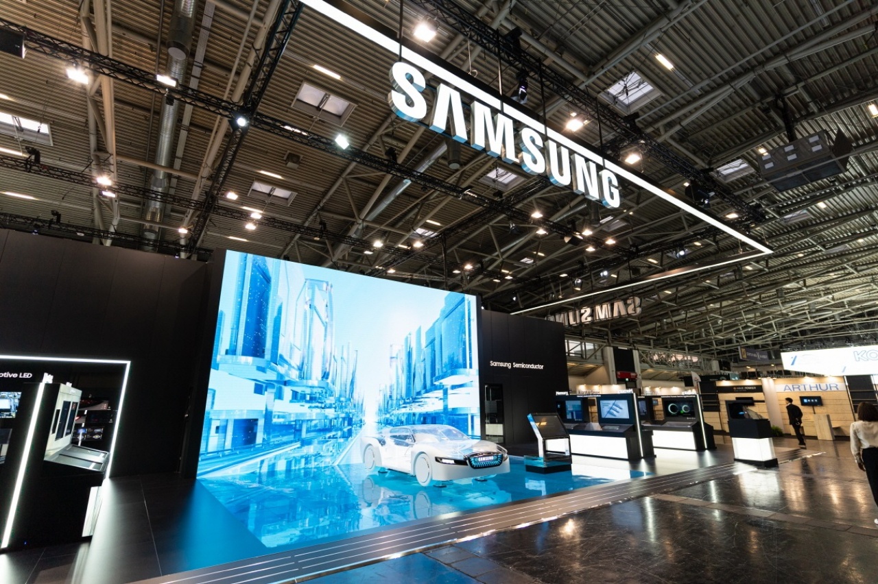
Samsung Electronics is setting up a new semiconductor research facility in Japan near Tokyo. The South Korean firm is reportedly spending $280 million or ¥40 billion on this project.
According to NHK Japan, Samsung Electronics will build its research and development (R&D) hub in the Minato Mirai business district located in the city of Yokohama. The site is expected to be a center for inventing chip-packaging technology for high-performance silicon.
Japanese Government's Subsidy Grant
It was reported that Japan has been continuously working on attracting foreign semiconductor companies so they will open their facilities in the country. This is because the nation sees chipmaking as critical to economic security and would like to boost its local supply chain.
As part of its efforts to entice chipmakers, the Japanese Ministry of Industry revealed it will grant subsidies to Samsung Electronics worth up to ¥20 billion. With this amount, the government covers almost 50% of the total cost of the new R&D facility.
Japan will continue to scale up its chip industry as it looks to support the recovery of domestic chip manufacturing. Prime Minister Kishida Fumio confirmed that the government committed to subsidizing Samsung Electronics for its advanced chip lab in the territory. In any case, Reuters reported that the electronics firm's $280 million investment is set to be distributed over five years.
Details About the New Samsung Research Center
Meanwhile, Korea Joongang Daily mentioned that Samsung Electronics' research center in Tokyo has been named the "Advanced Package Lab" or simply APL. The hub will have a floor space measuring 71,000 square feet and be divided to house the company's research facilities and backup offices. The firm aims to open the lab in 2024 and is expected to hire about 100 new researchers.
"Samsung wishes to fortify leadership in semiconductors through continuous technology research," Samsung's head of chip unit, Kyung Kye Hyun, said in a statement this week. "Yokohama is one of the most suitable locations to collaborate with industries, universities and research centers, as it houses many companies and institutions related to chip packaging."
Photo by: Samsung Media Library